TRANSISTORIZING THE T-368 EXCITER
An experimenter's notes... but not every detail
9/14/95
Copyright © 1995 by John Seboldt. Permission
granted
for further distribution for individual use of radio hobbyists only.
A few changes 6/10/2001
 This
project uses the existing tuned circuits, physical structure, and some
parts and wiring of the exciter from the old Collins military T-368
transmitter
as the basis of a solid-state VFO/multiplier for most of the HF region
of interest to amateurs.
This
project uses the existing tuned circuits, physical structure, and some
parts and wiring of the exciter from the old Collins military T-368
transmitter
as the basis of a solid-state VFO/multiplier for most of the HF region
of interest to amateurs.
[check J105/P105]
As supplied, it has a 1.5-3 MHz PTO, a mechanical
digital
readout, and doubler stages to cover 1.5-3, 3-6, 6-12, and 12-24 MHz
(they
say 12-20, but the dial reads to 24; probably reflects the ratings of
the
companion PA). It measures about 10" wide by 9" high by 11" deep, so
it's
not small, and as I received it there was no enclosure for the whole
assembly
-- no problem for less critical applications like HF, but probably best
to add shielding (I haven't yet for HF QRP!). It's built like a tank,
and
the tuned circuits in the multipliers track the PTO in typically
elegant
Collins fashion.
I got it from Fair Radio Sales, a renowned surplus
dealer,
about 5 years ago without the output tube (the 6000, a rare beast
nowadays).
It cost $35 then; one of my correspondents informs me that they now run
$45 without the output tube. I first used it as an improvement over a
Heathkit
HG-10 VFO with a DX-60 transmitter, and it was remarkably stable even
in
its tube form.
Once transistorized, you get an incredibly stable
VFO
for the home station that covers a wide range, complete with receiver
and
transmitter offset pots on the front panel. It's not a unit for
backpacking,
because of its solid, heavy construction. But that weight and bulk is
part
of what assures mechanical stability. The sheer size of the sealed PTO
assembly, plus the fact that the components were designed for the
higher
RF currents of the tube circuit, means that once you solid state the
thing,
you have rock-like stability. There's even a thermostat-controlled
heater
you can hook up around the PTO tuned circuits. True, the unit tunes
pretty
fast on the higher bands, but the gearing is so good that there is no
backlash.
The offset pots can help you zero in if your hand isn't too steady.
My sources for circuit concepts and building blocks:
ARRL Handbook
QRP Classics (ARRL)
W1FB's Design Notebook (ARRL)
W1FB's QRP Notebook (ARRL)
Solid-State Design for the Radio Amateur (ARRL)
Peter Anderson, KC1HR, "Transistorizing Surplus
VFOs",
QST, Feb. 1989, page 45-46 (in Hints and Kinks)
T-368 manual pages and schematic relating to
exciter.
On ordering, I asked only for the pages from the T-368 manual related
to
the exciter, and Fair Radio quoted me $10 at the time.
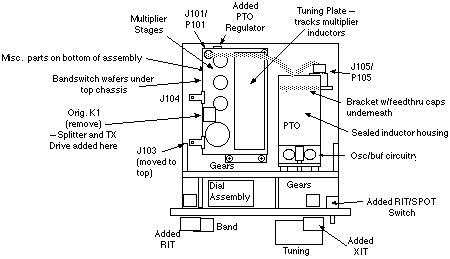
THE PTO
Removing the PTO takes some care -- you have to
loosen
not only the mounting screws, but the hex set screws on the PTO shaft
gear.
I suggest you set things at 3 MHz at the top end of the band, so you
know
where to reset things. All the electrical connections unplug, and all
these
wires are re-used, also the feedthrough capacitors attached to an
angled
bracket under the PTO. All the circuitry outside the tank circuit is on
a small sub-chassis under the tube sockets.
The original approach - transistorize existing circuit

I started with the QST article, which suggests using
2 40673 dual-gate MOSFETs. (The NTE222 is a currently-available
substitute
for the discontinued 40673 -- but they're about $5 each locally!). Read
this for some precautions about turning the PTO too far beyond its
range,
and damaging the internal slugs. I think it will go more than 50 kHz
beyond,
so you have some slop for recalibration. Also, the author warns not to
open the PTO sealed inductor can if you can avoid it -- the hermetic
seal
is one key to super-stability.
Having used various VFO circuits, I decided to save
a
few bucks, and used a plastic VHF JFET for the oscillator (NTE312 or
other
similar device). I took a 100 ohm resistor from regulated V+ (after the
existing RF choke) to drain; hooked drain to the original plate pin;
hooked
the gate to the original tube grid connection; and hooked the source to
the original cathode connection. A 1N914 diode goes from gate to ground
(cathode grounded). That author had put the diode from gate 1 to
source,
and this meant no oscillation for me without some kind of "kick", like
temporarily grounding the gate! When the diode went to ground like all
other oscillator circuits I've seen, all is well.
The tuning diode circuit provides an adjustment
range
for RIT/offset. These values gave me a tuning range of 7 kHz at the 3
MHz
end of the PTO when I tested it before re-installation. However, I
didn't
discover till I put things together that the tuning range at the bottom
end (near the 3.5 and 7 MHz ham bands) was substantially lower! At 80
meters,
I have barely enough to get an 800 Hz CW offset. At 40 meters, I even
have
only about +- 2 kHz.
I later put in an NTE618 tuning diode, designed for
AM
radio tuning service (440 pF at 1 volt!) Of course, I reduced the size
of the .01 uF capacitor iuntil the tuning range was reasonable. I think
it was about 100 pF, can't remember :-). Tuning range is about +/- 2
kHz
at 1.75 MHz, multiplying to +/- 16 kHz at the highest band.. My 10-turn
pots make even the widest range quite manageable. The stability is
SOMEWHAT
degraded by the tuning diode arrangement, but I still got less than 10
Hz drift overnight relative to WWV at 10 MHz.
I used a regulated 6 volt bus for the oscillator
(and
RIT bias -- see below), coming from a 3-terminal regulator mounted on
the
back of the multiplier. My regulator was an out-of-tolerance 7805; I'll
bet 5 volts from a good 7805 would be fine. T
The buffer is almost identical to the QST article
above,
except for output coupling and operation from a separate power bus.
Here
the original plate pin serves only as a tie point, the 10K plate
resistor
and 100 pF coupling capacitor being removed. Handle the MOSFET with all
due electrostatic precautions -- wrist strap, etc.
4 wires that enter the PTO circuit from the power
connector
are rewired as shown; the other two are for the VFO oven heater. You
should
not find this last option necessary, unless you are operating in the
Arctic!
At the feedthrough capacitors under the PTO, you have convenient points
to solder your connections to the rest of the assembly.
Re-installation of the PTO IS a bit tricky because
of
the split gear that eliminates backlash. You have to turn the one gear
so the springs are compressed, hold them in place with a screwdriver
until
you get them meshed with the gearing from the dial.
Later...
I just ripped out all the existing parts (in the
tube
compartment) and built the oscillator/buffer more cleanly, according to
the homebrew books.. The tuned circuit components to the left,
plus
the coupling capacitor, are the ones in the sealed can, and three pins
come into the tube compartment for ground, cathode/source, and
grid/gate.
Don't know exactly why I did this, other than to have less clutter in
there.
MULTIPLIER STAGES
I was on my own on the multiplier stages. It was
possible
to get some results by simply plugging in JFETs in the appropriate
places,
but little anomalies would creep in from the long wiring, old-style
"Vitamin
Q" bypass/coupling capacitors, etc. As I went on, I became less and
less
concerned with historic preservation, and more and more inclined to gut
the unnecessary parts.
On top of the chassis, rip out the relay K101,
intended
to switch between this exciter and an external one for FSK. Use the two
BNC connectors on angled brackets -- move both of them to the top, with
room for the power splitter /drive level pot.
Obviously JFETs are the best choice, to provide high
impedance
loads to the tuned circuits that were designed for tube grids. I used
the
NTE312 again.
FIRST VERSION: I just wired the gate to the grid pin
of
each stage (with a 47K resistor to ground), the drain to the plate pin,
and the source to chassis ground, clipping the existing grid resistors
to ground. Actually, the first stage has its gate (and associated
resistor)
going directly to the BNC connector from the VFO (J101). The plate
supply
wire was used, with its decoupling networks (1K series resistor and .01
uF capacitor to ground) . 1K, of course, is way too high for the
transistor
circuit, so I bridged something in the range of 68 to 100 ohms across
it.
They are on the bottom of the multiplier assembly -- three Phillips
screws
are accessible with a long screwdriver. The bandswitch and tuning
shafts
couple to the front panel with slotted plates to allow some free play,
so getting them back in takes some coordination. I got lots of practice
by taking it in and out many times!
The first stage works as a buffer on the low band,
and
a doubler above that. The low band switches in a load resistor instead
of the tuned circuit -- R106, 10K (on the bottom again!). This
obviously
needs to be lower. I plugged in different resistors (in the 3300 ohm
range,
can't remember) across this resistor, until the output at S101, pin 8
was
the same on bands 1 and 2.
The second multiplier stage had a tendency to
self-oscillate.
I cured it with a series RC network from gate to ground, in parallel
with
the gate resistor: 2200 ohms and 0.1 microfarad. This obviously loads
down
the tank circuit enough to reduce the Q. A resistor directly across the
appropriate tuned circuit might work as well; the series R-C method was
simply used because it was easiest to apply without taking the assembly
off a million more times. Another such network went on the input of the
third multiplier when I discovered another oscillation on the highest
band.
SECOND VERSION: Further reflection led me to dislike
the
sheer length of the unshielded bandswitch wiring in the original
circuit.
So, the little terminal board on the bottom was completely ripped out,
and replaced with a piece of double-sided PC board. Everything was
basically
re-wired as cleanly as possible near the new PC board ground plane,
with
excursions to the bandswitch being as direct as possible. The dog-bone
ceramic coupling capacitors between tuned transformer stages were saved
and re-used for "historical" reasons -- with some wire and insulating
tubing
to extend them, they were placed directly between the appropriate
tuning
cans, between the new PC board and the metal chassis. Also saved were
the
15 pF capacitors that had been placed near the tube grids, which are
part
of the overall tuning capacitance, apparently being placed nearer the
tube
grids to aid in bypassing?
The final tuned circuits were also used in this
second
rewiring. The lowest band tuned circuit was used as a tuned load for
the
first buffer/multiplier on the lowest band, and the output attenuated
with
resistors to match the output of the other bands. The others were
incorporated
into the circuit by means of 20 pF coupling capacitors. The slugs do
not
make much difference in the upper 3 bands, but overall waveform purity
seems to be better with these coupled in, so you might as well use them.
All of this fed into a broadband step-down
transformer,
wound on an FT-37-73 core, approximately 15 to 5 turns ratio (have to
look
again).
This yielded about 1 volt peak to peak output.
OUTPUT AMPLIFIER
FIRST VERSION: In the area of the IPA (intermediate
power
amplifier, another word for "driver") tube, I built a broadband buffer
stage based on W7ZOI's buffer in the VFO section of the "high
performance
communications receiver" project in the ARRL Handbook. Any broadband
buffer
circuit with a hi-Z input and a high output into 50 ohms would be
suitable.
The input comes right off S101, section 2, rear, pin 12.
 The
splitter transformer requires a 25 ohm input. When built separately,
the
splitter would be preceded by a 2:1 impedance transformer (approx. 4:3
turns ratio autotransformer). With an output transformer already
present,
just take some turns off the secondary (originally 5 turns).
The
splitter transformer requires a 25 ohm input. When built separately,
the
splitter would be preceded by a 2:1 impedance transformer (approx. 4:3
turns ratio autotransformer). With an output transformer already
present,
just take some turns off the secondary (originally 5 turns).
I got output of about 3V peak to peak into 50 ohms
on
the lower 3 bands, and 2V p/p on the highest. Pure sine waves are not a
concern for me, since diode ring mixers generate harmonics anyway, and
even would rather have a square wave. If it is for you, you can put in
a low pass filter for each band, using the S101 section 1 rear
(rewired)
to pick them.
SECOND VERSION: I used a broadband output amplifier
based
on a 2N3866 (from DeMaw's "W1FB's Design Notebook"), with adjustable
gain
(pot in place of the emitter resistor). This gave me about 4 volts p-p
on the low end, about 3 volts at the upper limit. This is enough to
accomodate
any combination of splitters, high-level diode mixers, or what have you.
FOR FUTURE EXPERIMENTING: Consider also some CMOS
chips
as output amps. A recent QST article featured 74HCxxx chips to put out
nice clean 5 volt P-P square waves. There is no better driving signal
for
diode ring mixers.
FINAL ALIGNMENT: Make the best compromise you can
between
uniformity of output in a given band, and waveform purity (least
feedthrough
of sub-harmonic signals). This will take some head-scratching and
fiddling,
but you can do it.
OFFSET TUNING -- TRANSMIT AND RECEIVE
I have two pots (found matching knobs at a local
surplus
house!) and a switch added to the front panel, and a transistor
switching
arrangement (built on the pot terminals) to select the correct pot when
the transmitter is keyed. I used 2000 ohm 10-turn pots -- you can use
probably
use anything from 2 to 10K. You can fiddle with resistors on either
ends
of the pot(s) to limit tuning to the most linear part of the varactor's
range if you wish.
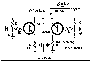 The
capacitors hold the VFO at the transmit frequency until the CW waveform
has decayed to zero. Your mileage may differ as far as the values
needed.
The
capacitors hold the VFO at the transmit frequency until the CW waveform
has decayed to zero. Your mileage may differ as far as the values
needed.
Remember that the diodes affect temperature
stability
-- as the temperature goes up, the voltage drop goes down, reducing the
output voltage and lowering the frequency. If you're lucky, this
compensates
for the temperature characteristics of the varactor diode! For all I
know,
the transistors behave similarly. Thus you might best place them near
the
VFO in a small enclosure. I've gotten by with being sloppier, and the
thing
is still more stable than you can imagine.
The SPDT switch (front panel) attaches the key lines
either
to the system keying line, or directly to ground. When grounded, you RX
and TX on the same frequency for SSB or for spotting a CW signal to
zero
beat. When in the other position, you have receive offset for a CW beat
note, or for RIT in SSB or CW.
John Seboldt K0JD
Milwaukee, WI (but "forever a zero", having moved out
of zero-land for the first time in 1999)
k0jd
at seboldt dot net
THE AUTHOR:
John
Seboldt, K0JD, began hamming as WN0QXG in about 1967. Music,
electronics,
and ham radio grew side by side in his youth, leading to work in the
broadcast
industry while studying music at Luther College, Decorah, IA, and The
University
of Iowa, Iowa City. Church music has been his main field -- he served
15 years
in the Twin Cities, and moved to Milwaukee in 1999. (Check out samples
of his music work at www.seboldt.net/annunciation).
For now, technology has again claimed his working hours: at Time Warner Cable he's a
Broadband Technician, having worked in the cable industry since 2001.